Observation and 3D Measurement of Cream Solder Application Conditions
Cream solders, or solder pastes, connect and bond a surface-mount device (SMD) with a board in surface-mount technology (SMT), the method most widely used for PCB mounting. The cream solder printing or application conditions greatly affect the quality of PCBs. This section introduces basic solder knowledge, the PCB mounting process, and the latest examples of observation and measurement of cream solders that play an important role in evaluation for quality assurance, research, and development of these solders.
- Basics of Solders
- Characteristics of Cream Solder and Other Solders
- Steps in Reflow Soldering and Other Soldering Methods
- Examples of Observation and 3D Measurement of Cream Solder Application Conditions
- A 4K Digital Microscope That Improves the Sophistication of Cream Solder Observation and Analysis and Speeds Up the Operations
Basics of Solders
Solders are metal bonding materials used for connecting electronic components to a PCB. Typical solders melt at less than 450°C. They are alloyed with copper at joints on a PCB and bond a contact when hardened. Bonding using solders is called soldering.
Typical soldering uses a flux to increase the permeability and wettability* of solders. Fluxes are made from botanical resin such as rosin. Fluxes have some other effects, such as preventing oxidisation during heating and chemically removing oxidised films and dirt from the metal surfaces.
Conventional solders (eutectic solders/lead-based solders) include approximately 40% lead (they include 63% tin and 37% lead). With a melting point of 183°C, these solders are heated to approximately 250°C for bonding in typical applications. However, because lead has a serious impact on the environment when disposed of as industrial waste, lead-free solders have been the most common material since around 2000. To use lead-free solders, the heating temperature needs to be set approximately 30°C higher than conventional solders. For this reason, the temperature profile setting for the reflow process is important in reflow soldering, which is the most common method used for surface mounting. This widespread use stems from the fact that mounting can be defective on PCBs warped by excessive heating. Lead-free solders have wettability lower than conventional solders, which may cause a defect called solder balls depending on the applied cream solder conditions or temperature control in the reflow process. Solder balls can cause circuit defects or malfunctions.
- TipsWhat is wettability?
- Wettability in soldering is also called solder wettability. Wettability is the ability of melted solder to spread on a contact surface instead of being repelled. Solder wettability greatly affects the bonding strength. For example, if a solder hardens without sufficiently spreading onto the land or pad on a PCB due to insufficient wettability, the mounted device may have problems such as lower bonding strength, poor contact, and poor conductivity, resulting in equipment failures.
-

- It can be said that the wettability is higher when the contact angle θ (A in the figure) is closer to zero degrees. For soldering, higher wettability results in increased bonding strength between the board and the mounted components. An extremely high contact angle θ (low wettability) can cause mounting defects and, if the cream solder spherically hardens, generate solder balls that can cause short circuits. To prevent these problems, it is important to check the wettability of the cream solder on lands before use in automated mounting processes, especially the reflow process.
Characteristics of Cream Solder and Other Solders
Cream solder, also called solder paste, is a pasty solder made from powdered solder and flux.
Cream solder is used for SMT, which is most commonly used currently. In mass production, cream solder is applied to lands on a PCB via silkscreen printing and heated in furnaces to solder SMDs.
In some applications, dispenser robots and inkjet printers are used to apply cream solder in specified patterns.
Other typical solder forms
In addition to cream solder, typical solder forms include the following. This section explains the characteristics of and how to use them.
- Wire solder
- Wire solder looks like a wire. Wire solder contains flux threads. A soldering iron is used to directly heat and melt wire solder to solder SMDs on a PCB. Wire solder is fed by an automatically controlled soldering machine.
- Solder bar
- This form of solder is used for insertion mount technology (IMT) in which leads or electrodes are inserted into through-holes on a PCB and soldered. Solder bars are melted in a solder bath and used for soldering.
Steps in Reflow Soldering and Other Soldering Methods
Reflow soldering is the most commonly used method in the automated mounting process using SMT.
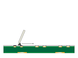
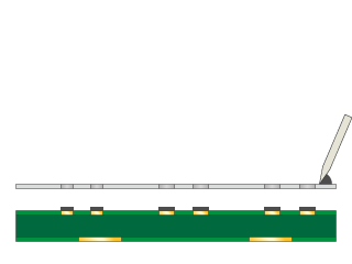
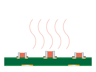
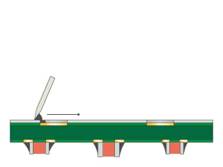
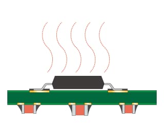
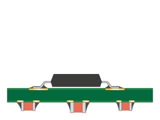
In typical reflow soldering, cream solder is applied to lands on a PCB in specified patterns through metal masks by screen printing. Adhesives are also applied to the specified patterns to hold the SMDs that are automatically mounted on the patterns by the mounter. The PCB is put into a reflow furnace and heated to bond the SMDs. This process is called the reflow process.
SMDs can be mounted on the other side of the PCB by turning it over. Cream solder is applied on the other side of the PCB and SMDs are mounted on it. The PCB is heated again in the reflow furnace. The process is shown in the following figures.
Other typical soldering methods
In addition to reflow soldering, there are various other soldering methods. The following are typical methods used for soldering such as manual soldering, automatically controlled soldering, and automatic soldering in lines.
- Soldering using an iron
- The tip of the soldering iron is heated to a high temperature using a nichrome wire heater or ceramic heater and is brought into direct contact with solder wire to heat it. SMDs are bonded to a PCB using melted solder wire. Some soldering irons have a highly useful temperature adjustment function to match the temperature to the melting temperature of the solder to use. In addition to manual soldering, soldering irons are also used in automated soldering machines. Some applications use portal frame equipment or robot arms equipped with soldering irons to solder SMDs precisely to the coordinates programmed by automatic control.
- Flow soldering
- The lower surface of a PCB is brought into contact with the liquid solder surface, which is melted solder bars, in a solder bath to solder SMDs on the PCB. This method is mainly used for mounting dual in-line packages (DIP) having leads. There are two types of soldering baths used for flow soldering: the static bath, which keeps liquids at rest, and the jet wave soldering bath, which creates waves on the liquid solder surface.
Examples of Observation and 3D Measurement of Cream Solder Application Conditions
When cream solder, made from powdered solder and flux, is printed on or applied to lands, its wettability greatly affects the mounting quality and reliability. Wettability of applied cream solder can be evaluated with the angle to the land. It is also important to observe the appearance and measure the volume and shape of cream solder to determine how powdered solder and flux spread onto the land.
It is, however, difficult to bring the cream solder into focus throughout the entire field of view for observation due to glare from light reflection, light reflectance different from that of the background, and shapes having height differences. It is also impossible to measure the shape of cream solder using contact-type measuring instruments before reflow soldering. Additionally, it is difficult to measure the dimensions of 3D shapes precisely using optical microscopes.
KEYENCE’s VHX Series 4K digital microscope uses an optical system and a 4K CMOS image sensor that provide both a large depth of field and high resolution and a system including highly functional lighting and sophisticated image processing. With these features, condition determination and focus adjustment on three-dimensional targets are no longer difficult, requiring only simple operations. The result is clear observation with high-resolution 4K images. Additionally, non-contact, highly accurate 2D and 3D measurement can be performed with high-resolution 4K images used for the observation. Read on for examples of VHX Series observation and measurement of cream solder applied to lands on a PCB.
High-resolution observation of cream solder with 4K images
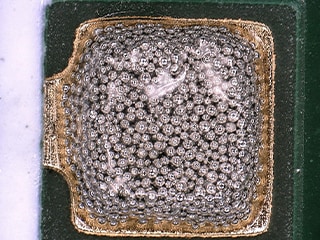
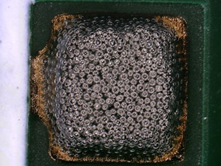
Thanks to a large depth of field, the VHX Series 4K digital microscope can capture fully focused clear images of three-dimensional cream solder applied to lands. The ring-reflection removal function and glare removal function can be used to eliminate the effects of light reflection specific to cream solder. These functions enable observation using a high-resolution 4K image that clearly shows the details of cream solder such as conditions of microscopic powdered solder and flux and boundaries between the lands and cream solder.
Additionally, lighting conditions can now be determined at the press of a button. Using the Multi-lighting function, which automatically obtains data of images captured with lighting from all directions, observation can be started simply by selecting a suitable image. Image data obtained under each lighting condition is stored. Operators can observe the target data at a later day from different perspectives by selecting an image captured under different lighting conditions. Simply select an arbitrary image to reproduce the conditions used to capture that image. The observation can be resumed promptly on a different sample of the same type of target on a later day under the same conditions.
3D measurement and profile measurement of cream solder
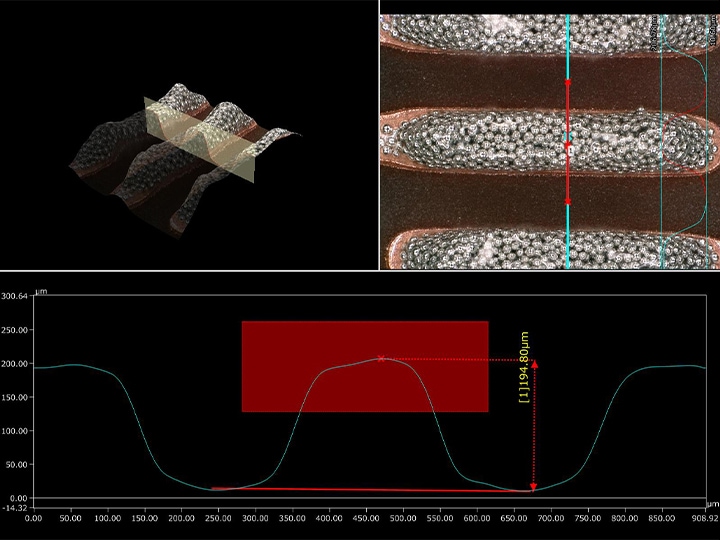
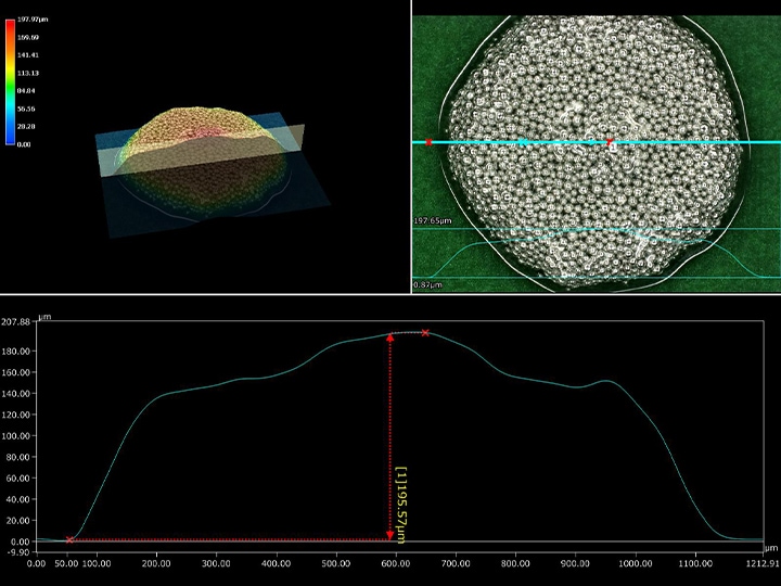
The VHX Series 4K digital microscope can create a 3D image that shows changes in microscopic texture and surface roughness using a clear 4K observation image captured from directly above. These images allow for quick and highly accurate 2D and 3D measurement.
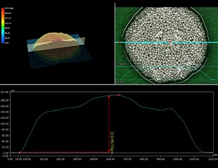
This function also enables non-contact 3D and shape measurements (including height and volume of cream solder), which are difficult with contact measuring instruments. Causes of solder defects, such as an insufficient amount of application and cold joints, can be quantitatively evaluated based on the volume and shape of cream solder.
Operators can also measure profiles by simply specifying the desired location with a mouse while watching the screen. Two-dimensional sectional shapes of cream solder applied in various shapes can be measured in a non-contact, non-destructive manner, which is useful when, for example, wettability is evaluated based on the angle to lands.
A 4K Digital Microscope That Improves the Sophistication of Cream Solder Observation and Analysis and Speeds Up the Operations
As PCBs and devices are becoming increasingly smaller and denser, manufacturers in the electronic device industry are competing globally with each other to ensure high quality and create new technologies. The functions and performance of the VHX Series 4K digital microscope eliminate various problems and are accessible quickly with simple operations, allowing you to maintain your high competitive edge in the electronic device industry.
The VHX Series can perform clear observation at high magnifications with 4K images; creates highly accurate 3D images; measures two dimensions, three dimensions, and profiles; and automatically creates reports, all seamlessly with a single unit, greatly increasing the accuracy and speed of evaluation for research, development, and quality assurance.
For additional info or inquiries about the VHX Series, which can significantly improve a wide range of observation and analysis tasks in the manufacturing of electronic devices such as PCs, click the buttons below.


