Observation and Measurement of Semiconductor Wafers and IC Designs Using Microscopes
There has been intense competition in the semiconductor industry to produce smaller and more functional products, improve productivity, and reduce costs. In response to increasingly smaller designs and larger diameter wafers, more advanced quality assurance and even faster R&D and inspection continue to be required.
This section introduces new application examples of KEYENCE’s latest 4K Digital Microscope, which makes inspections in the semiconductor industry much more advanced and efficient.

- Larger Diameter Wafers and New Requirements
- Latest Solutions for Inspection of Wafers and IC Designs
- Observation of wafers using 4K Optical Shadow Effect Mode
- Observation and measurement of wafer edges
- Observation and analysis of defects that occur in wafer processing
- Observation and 3D shape measurement of foreign particles adhering to a wafer
- High-resolution observation of IC patterns
- Overall image observation and magnified observation of IC patterns
- 3D shape measurement of IC patterns
- The VHX Series, a New Powerful Partner in the Semiconductor Industry
Larger Diameter Wafers and New Requirements
Wafers are indispensable in the manufacturing of semiconductors. To be used in increasingly smaller devices, semiconductor products are required to be more compact but have higher functionality and quality. To manufacture value-added products effectively, many manufacturers are competing against each other in the areas of research and development, development of manufacturing technologies, and quality control.
One popular example to increase productivity is to produce larger diameter silicon wafers so as to produce many chips from a single wafer. The production of larger diameter wafers has been studied for many years to meet various requirements such as reduced loss due to defects, higher flatness, and lower costs. To produce larger and flatter wafers, double side polishing is considered to have advantages over single side polishing, and thus double side polished wafers with a diameter of 12 inches are most widely produced. Wafers with a diameter larger than 12 inches have appeared in recent years, and wafers with a diameter of 15 inches or even larger are expected to be produced in the future. To ensure stable quality of such wafers and further increase productivity of IC chips, constant research and development is crucial.
The popular circuit patterning technologies include high-definition screen printing, which efficiently prints patterns fine enough to be used in micro-electromechanical systems (MEMS), and inkjet coating (inkjet printing), which enables efficient small-volume manufacturing of many product types and quick prototyping and testing through a technique for patterning with ink according to the data instead of using photomasking. Given this background, more accurate and swift observation, inspection, and evaluation are required.
Latest Solutions for Inspection of Wafers and IC Designs
To provide a more highly advanced observation environment, KEYENCE has repeatedly improved its digital microscopes for the past 30 years using direct customer feedback. The latest technologies including 4K resolution have brought about a major evolution in KEYENCE’s digital microscopes, and the result is our latest microscope, the VHX Series high-definition 4K Digital Microscope.
This section introduces inspection examples of wafers and IC designs using the VHX Series, which enables high-magnification observation and analysis with clear high-resolution 4K images, as well as various inspections including 2D and 3D measurements and automatic area measurement. All examples introduced here use a single VHX Series unit.
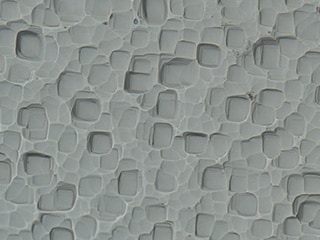
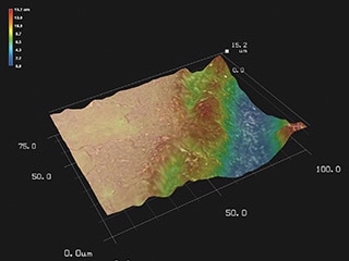
Observation of wafers using 4K Optical Shadow Effect Mode
Using a specialised design featuring a high-resolution lens, a 4K CMOS image sensor, and lighting technology, the VHX Series 4K Digital Microscope has achieved a whole new method of microscopy, “Optical Shadow Effect Mode.”
The multi-directional lighting variation method analyses the contrast on the image captured with varied illumination, allowing users to detect subtle irregularities on a target. Even subtle irregularities on a wafer can be clearly observe.
Colour information can be overlaid on the Optical Shadow Effect Mode image, enabling simultaneous representation of the uneven surface and colour information. Images are easier to interpret with a height colour map.


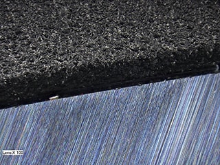
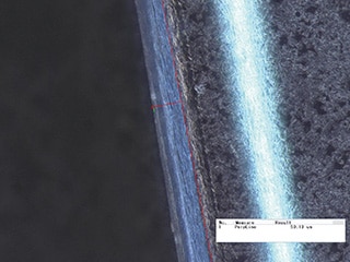
Observation and measurement of wafer edges
The free-angle observation system of the VHX Series 4K Digital Microscope enables tilted observation of wafer edges.
The deep depth of field and the real-time depth composition make it possible to obtain clear high resolution images that fully focus on the entire surface, edges, and defective areas of a wafer even at high magnification.
The created high-resolution magnified image can also be used for highly accurate 2D measurement and 3D shape and profile measurements of defective areas. These measurements make it possible to complete procedures quickly and seamlessly with a single unit.

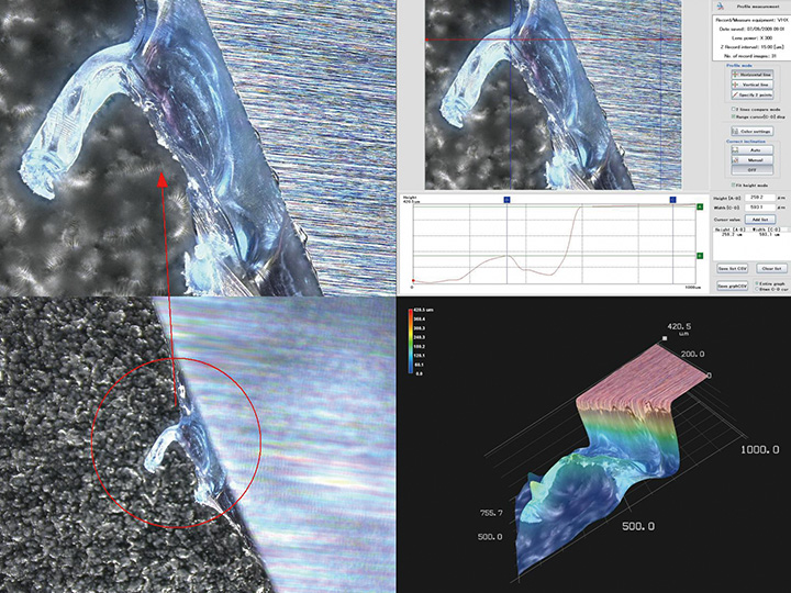
Observation and analysis of defects that occur in wafer processing
The VHX Series 4K Digital Microscope has a deep depth of field. In addition, its high-dynamic-range (HDR) imaging function captures multiple images at varying shutter speeds to obtain an image with high colour gradation and contrast. Microscopic defects can be analysed quickly with simple operations even on highly reflective targets having almost no contrast.
3D imaging that enables 3D shape measurement does not require many images, and a height colour map allows users to obtain and analyse measured values of the topography of the defect. Furthermore, with the automatic area measurement tool, photomasking can be measured and measured values and a histogram of the measured area can be displayed, thereby dramatically improving work efficiency.


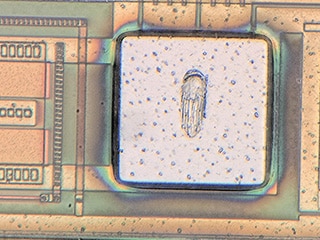
Observation and 3D shape measurement of foreign particles adhering to a wafer
The VHX Series 4K Digital Microscope supports high magnifications up to 6000x, thereby enabling the capturing of high-resolution images. These images enable, directly from high-magnification observation, submicron-order, highly accurate 3D shape measurement of microscopic foreign particles adhering to a wafer. Profile measurement is also possible on the desired cross section of the foreign particle. Such measurement allows users to complete the operations from advanced observation to measurement with a single microscope. Furthermore, the automatic area measurement and counting functions enable automatic contamination analysis.
In response to customer requests, KEYENCE can propose and integrate separate systems. A loader function, of course, can be added.

For details on the VHX Series and its lineup of products, click the button shown below to download the catalogue.
For information on other products and separate systems, feel free to contact KEYENCE by clicking the “Contact / Inquiries” button below.
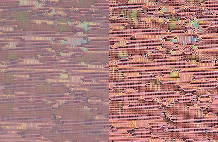
High-resolution observation of IC patterns
The VHX Series 4K Digital Microscope is equipped with a high-resolution lens and a 4K CMOS to enable high-resolution imaging. Microscopic IC designs can be observed with a high resolution 4K image.
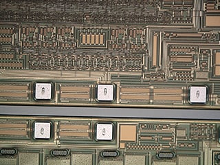
Overall image observation and magnified observation of IC patterns
The high-resolution lenses and the motorised revolver of the VHX Series 4K Digital Microscope enable a seamless zoom function that automatically switches lenses from 20x to 6000x magnification with intuitive operations.
The VHX Series also has a real-time composition function, which always provides a fully focused high-resolution image wherever users view in high-magnification observation. Simply click on the area to view to make this function automatically move the stage to the selected location and perform depth composition. You can observe subtle irregularities on IC patterns on a clear high-magnification image while tracking where you view.
Furthermore, at the push of a button, high-speed image stitching automatically stitches high-magnification, high-resolution images with no misalignment, providing a fully focused overall image of a large area with up to 50,000 x 50,000 pixels immediately. The VHX Series supports various observation applications quickly with easy operations.
3D shape measurement of IC patterns
The VHX Series 4K Digital Microscope instantly creates a fully focused image of IC patterns having irregular surfaces by composing multiple images with varying focus positions. When displayed in 3D, the IC pattern surfaces can be observed freely from various angles.
High-accuracy profile measurement can also be performed using the obtained height data, significantly improving inspection accuracy and work efficiency.

The VHX Series, a New Powerful Partner in the Semiconductor Industry
In addition to the functions introduced here, the VHX Series high-definition 4K Digital Microscope is equipped with many more useful functions for research and development and manufacturing sites. For semiconductor wafers and integrated circuits, a single unit is able to identify defects, capture images, perform 2D and 3D measurements, and automatically create reports.
Advanced automatic control and image processing allow even beginners to capture clear images quickly with simple operations. This dramatically improves both inspection accuracy and work speed.
For details on the VHX Series, click the button shown below to download the catalogue. For inquiries, click the other button shown below to contact KEYENCE.
